AMD Radeon RX Vega Prototype Makes 3DMark Fire Strike Appearance With 1.2GHz Core Clock
There are many questions surrounding AMD's next generation GPU architecture known as Vega, most of which have to do with performance. Those will be answered definitively soon enough. In the meantime, teases and leaks continue to give us glimpses of what to expect from Vega. The latest leak comes from what appears to be a prototype Radeon RX Vega card flexing its muscles in Futuremark's 3DMark Fire Strike benchmark.
The device ID is listed as 687F:C1. That points to an early Vega 10 prototype, the same one AMD brought to the Consumer Electronics Show (CES) earlier this year and used in a demo showing Doom running at 4K at Ultra settings. The prototype card ripped over 60 frames per second in that demo, sometimes even hitting 70 fps. Not too shabby when you consider the resolution and high level of eye candy involved.

We were on hand at CES and saw this for ourselves. Shown above is a screen capture of the video we took. That is not a cherry-picked screen capture, either—we did not witness any slowdowns or stuttering during the demo, which left us excited about Vega's potential.
Well, fast forward to today and that prototype card seems to have revealed itself in a 3DMark Fire Strike run. According to 3DMark's listing, this particular Radeon RX Vega card sports 8GB of onboard memory (presumably second generation high bandwidth memory, otherwise known as HBM2) running at 700MHz with the GPU clocked at 1,200MHz.

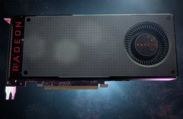
Click to Enlarge
According to 3DMark's listing, the Radeon RX Vega is plugged into an Asus Prime X370-Pro motherboard with a Ryzen 7 1800X processor running at stock clocks. That combination resulted in a Fire Strike score of 14,412, which 3DMark lists as being better than 84 percent of all results. The graphics score is 17,801. That is about 1,400 points higher than a Radeon R9 Fury X. it is also roughly equivalent to NVIDIA's Maxwell-based GeForce Titan X, and a couple hundred points shy of a GeForce GTX 1070.
This is a promising start for Vega. Bear in mind that this appears to be the same early prototype that AMD's been showcasing for months. Final silicon is bound to feature improvements, and perhaps a faster GPU clockspeed as well (1,200MHz is not all that exciting). Paired with more polished drivers with Vega releases, this particular SKU could be a real force in the graphics space—likely at least as good as the GTX 1070, and perhaps more in line with a GTX 1080, depending on what enhancements AMD is able to make.
It is always a good idea to temper expectations, though if you're looking for reason to be optimistic, almost everything we've seen from Vega up to this point has been positive. One of the more recent leaks came from a Linux driver and broke down the specs. If that information is correct, Vega will feature 64 next generation compute units, each with 64 GCN stream processors. That gives it 4,096 next generation GCN stream processors divided into four divisions, each of which comprises a shader engine.
To break things down even further, each 1,024 stream processor shader engine wields two asynchronous compute units, a render back-end, and four texture blocks. Inside each of those texture blocks are 16 texture mapping units, giving the graphics card a total of 256 TMUs. It also supports eight hardware threads.
Straight to the point, Vega is looking like it will make AMD competitive again in the high-end graphics market.