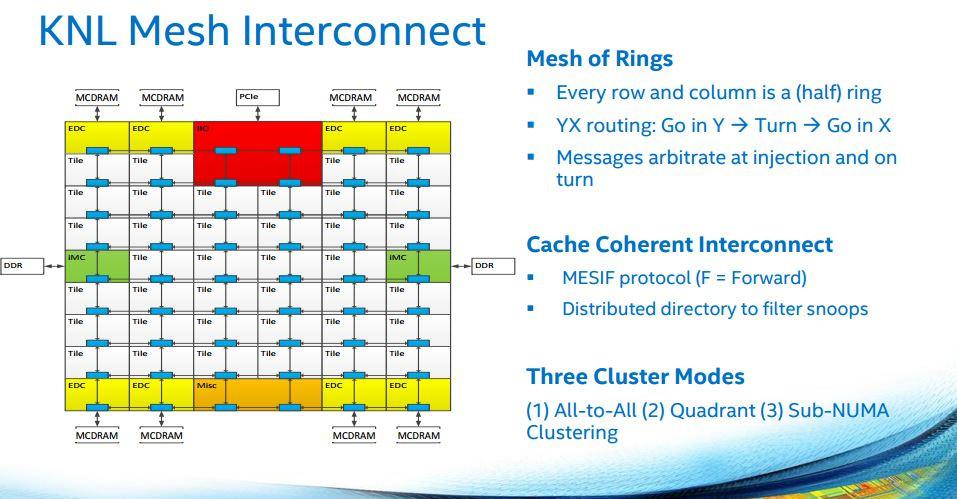
Intel is using a new Mesh Interconnect For Xeon, but also Skylake-X Processors. The 2010 ring-bus design is a thing of the past. The new mesh design allows communication in the several processor parts on an X/Y routing manner, moving though the grid, lowering latency.
Ring bus made and entry with Sandy Bridge generation processors back in 2010. Intel had desktop CPUs up to 4 cores and server models up to 8 cores. The ring bus made it relatively easy for Intel to design chips with more or less cores, because additional chips associated with it could insert a piece of L3 cache as a slice into a chip design. The ring bus connected all parts of the chip to each other. Data can be sent over a bidirectional track from one chip component towards another.
The task of adding more cores and interconnecting them to create a multi-core data center processor may sound simple, but the interconnects between CPU cores, memory hierarchy, and I/O subsystems provide critical pathways among these subsystems necessitating thoughtful architecture. These interconnects are like a well-designed highway with the right number of lanes and ramps at critical places to allow traffic to flow smoothly rather than letting people and goods sit idle on the road without being productive.
Increasing the number of processor cores and raising the memory and I/O bandwidth per processor to service the demand for a wealth of data center workloads produces several challenges that must be addressed through creative architectural techniques. These challenges include:
- Increasing bandwidth between cores, on-chip cache hierarchy, memory controller, and I/O controllers. If the available interconnect bandwidth does not properly scale with other resources on the processor, then the interconnect becomes a bottleneck limiting system efficiency like a frustrating rush hour traffic jam.
- Reducing latency when accessing data from on-chip cache, main memory or other cores. The access latency is dependent on the distances between the chip entities, the path taken to send requests and responses, and the speed at which the interconnect operates. This is analogous to commute times in a spread out vs compact city, number of available routes, and the speed limit on the highways.
- Creating energy efficient ways to supply data to cores and I/O from on-chip cache and memory. Because of the larger distances and increased bandwidth requirements of each component, the amount of energy spent for the data movement to complete the same task goes up when more cores are added. In our traffic example, as a city grows and commute distances increase, the time and energy wasted during the commute leaves less resources available for productive work.
Intel is committed to innovating architectural solutions to stay ahead of these challenges in creating more powerful and efficient processors to meet the demands of established and emerging workloads such as artificial intelligence and deep learning.
Intel has applied its experience and innovation in developing a new architecture for the upcoming Intel Xeon Scalable processors to provide a scalable foundation for the modern data center. This new architecture delivers a new way of interconnecting on-chip components to improve the efficiency and scalability of multi-core processors (but also Skylake-X)
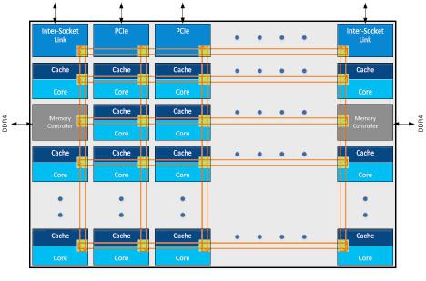
The Intel® Xeon® Scalable processors implement an innovative “mesh” on-chip interconnect topology that delivers low latency and high bandwidth among cores, memory, and I/O controllers. Figure 1 shows a representation of the mesh architecture where cores, on-chip cache banks, memory controllers, and I/O controllers are organized in rows and columns, with wires and switches connecting them at each intersection to allow for turns. By providing a more direct path than the prior ring architectures and many more pathways to eliminate bottlenecks, the mesh can operate at a lower frequency and voltage and can still deliver very high bandwidth and low latency. This results in improved performance and greater energy efficiency similar to a well-designed highway system that lets traffic flow at the optimal speed without congestion.
The scalable and low-latency on-chip interconnect framework is also critical for the shared last level cache architecture. This large shared cache is valuable for complex multi-threaded server applications, such as databases, complex physical simulations, high-throughput networking applications, and for hosting multiple virtual machines. Negligible latency differences in accessing different cache banks allows software to treat the distributed cache banks as one large unified last level cache. As a result, application developers do not have to worry about variable latency in accessing different cache banks, nor do they need to optimize or recompile code to get a significant performance boosts out of their applications. The same benefit of uniform low latency accesses carry over to memory and IO accesses as well and a multi-threaded or distributed application with interaction between executions on different cores and data coming from IO devices need not have to carefully map cooperative threads on the core within a single socket to get optimal performance. As a result such applications can take advantage of larger number of cores and still achieve good scalability.