IEDM 2017: Intel unveils 10nm technology

It has taken longer than expected, but three years after Intel unveiled its 14nm technology at IEDM and nearly one year after it demonstrated a Cannon Lake laptop at CES, the company is finally ready to discuss its 10nm process in detail. In a talk at this year's conference, Intel explained how it has for the first time packed 100 million transistors in one square millimeter of die area--which it said is the densest CMOS transistor density to date--and increased performance.
The basic features of the 10nm technology have been known since Intel's Technology and Manufacturing Day earlier this year. The space between the fins measures 34nm, the gate pitch measures 54nm, and the minimum metal pitch is 36nm. Intel continues to scale the SRAM cell size by 0.5x with each generation since 180nm and the smallest cell at 10nm measures 0.0312 square microns. These dimensions are similar to those of the competing 7nm processes from the leading foundries that manufacture chips for fabless customers such as Apple, Nvidia and Qualcomm.
At IEDM, Intel provided more details on the manufacturing steps, features and materials. The 10nm process is based on Intel's third generation of 3D transistors, first introduced at 22nm and known as FinFETs because the channel of 'fin' sits on top of the substrate with multiple gates wrapped around it. The thinner and taller the fin, the better the performance. At 10nm, the fin is just 7nm wide and 46nm tall (the latter is interesting because Intel had previously said that the 10nm fin measured 53nm). The fin height is also 'tunable' within a range of plus or minus 5nm depending on the application.
This aggressive scaling with standard 193nm immersion lithography tools is enabled by introducing a multi-patterning process known as Self-Aligned Quadruple Patterning (SAQP) to create the fins, a process that adds four additional steps in exchange for higher density. Intel is also using fewer fins in the standard cell and introduced two new tricks to further increase the density. The first was to eliminate a dummy gate at boundary of active cells. The second, known as Contact Over Active Gate (COAG), lands the vias directly on the top of active gate area, a technique that requires three extra steps but delivers a 10 percent reduction in cell area.
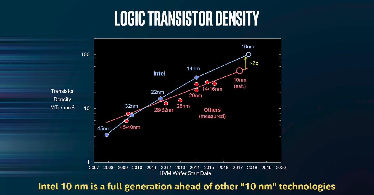
In the past, Intel has referred to these additional measures by the somewhat gimmicky name of 'hyperscaling,' but the bottom line is that density is scaling at or even beyond historical rates. Based on Intel's new metric, which it said is a more accurate measure of the density of modern processors that primarily consist of random logic, the rate of density increase of Intel's technology as actually been accelerating from twice the transistors per generation from 45nm through 22nm to 2.7x at 14nm and now 10nm.
It is important to note, however, that Intel is not plotting this over time. Intel has abandoned its tick-tock cadence and it is taking longer to get to each new generation, so over time Intel is roughly in line with the doubling of transistor density every two years, according to Chris Auth, a vice president in Intel's Technology and Manufacturing Group and Director of Advanced Transistor Development.
The tighter fin pitch, Intel's latest generation of strained silicon, and contacts with lower resistance (in part by replacing tungsten metal with cobalt) deliver higher transistor performance. Intel had previously said that in comparison to 14nm, 10nm would deliver a 25 percent increase in performance or cut power nearly in half. At IEDM, the company said 10nm increases drive current by 71 percent for NMOS transistors and 35 percent for PMOS.
The interconnects include 12 metal layers and support multiple voltages for different applications. Intel is using SAQP at the two lowest metal layers (M0 and M1) and SADP (double-patterning) at the next four layers to maximize density. It has also swapped copper for cobalt at the M0 and M1 layers to reduce resistance and improve reliability.
What Intel did not say is when exactly the first 10nm processors will be available (the IEDM paper states that it has demonstrated yield on its 204Mb SRAM test chip and on microprocessors, without providing any further details). The first 10nm family, known as Cannon Lake, should show up in laptops in early 2018. This will be followed by a 10+ process, used for a processor family code-named Ice Lake, and a 10++ process that will further boost performance.