Intel took half a day this week to talk about processor manufacturing technology. The company still believes in Moore's Law and says the principle will continue to guide and shape the microchip industry. But the way the law works is changing. The company also wants to change how people talk about manufacturing processes, because current terminology—wherein the node size is used to characterize a particular process—no longer serves as a good guide to how many transistors can be packed into a chip.
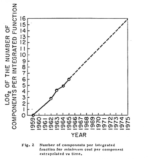
Moore's Law—the observation by Intel co-founder Gordon Moore that the number of transistors in an integrated circuit would double every two years, and correspondingly, the cost per transistor would halve over the same time frame—guided microchip manufacturing for around three decades. During that period, process node shrinks, each one bringing a doubling of the number of transistors by making everything 0.7 times smaller, were all it took to fulfill Moore's Law. Backed by this easy scaling, computer performance increased at a rate unrivaled by any other human technological innovation.
This scaling started to falter in the 2000s when it became increasingly difficult to shrink integrated circuits simply by switching to a smaller process node. But this didn't bring about an end to Moore's Law; instead, the industry used additional techniques, such as strained silicon, high-κ metal gates, and FinFETs. The doubling of transistor density or halving of transistor cost continued to take place every two or so years.
Intel's most recent process shrinks, however, have taken an extended period. The company introduced 14nm in September 2014 with the Broadwell processor. Its latest Kaby Lake processors are still built on a 14nm process, and although 10nm processors are due to ship this year, a fourth generation of 14nm chips, Coffee Lake, is also planned.
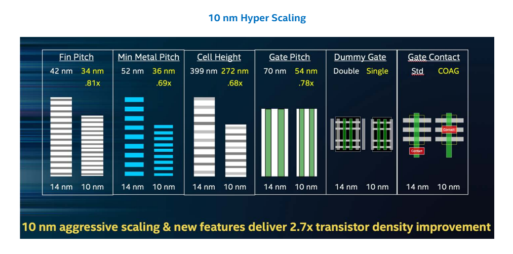
On the face of it, three years between process shrinks, rather than the traditional two years, would appear to end Moore's Law. But Intel claims that's not so. The company says that the 14nm and 10nm process shrinks in particular more than doubled the transistor density. At 10nm, for example, the company names a couple of techniques that are enabling this "hyperscaling." Each logic cell (an arrangement of transistors to form a specific logic gate, such as a NAND gate or a flip flop) is surrounded by dummy gates: spacers to isolate one cell from its neighbor. Traditionally, two dummy gates have been used at the boundary of each cell; at 10nm, Intel is reducing this to a single dummy gate, thereby reducing the space occupied by each cell and allowing them to be packed more tightly.
Each gate has a number of contacts used to join them to the metal layers of the chip. Traditionally, the contact was offset from the gate. At 10nm, Intel is stacking the contacts on top of the gates, which it calls "contact over active gate." Again, this reduces the space each gate takes, increasing the transistor density.
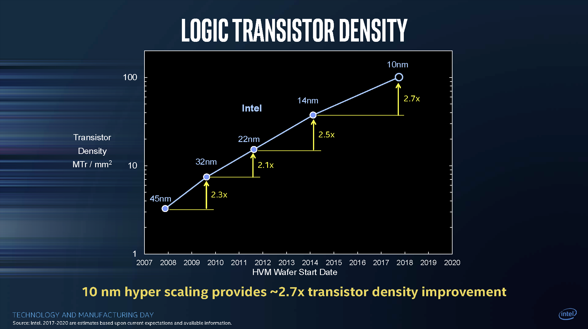
These additional features, Intel says, make up for the increased time between process shrinks. So while the company might only manage two process in the five and a half years following the introduction of 22nm (rather than the traditional almost three), Intel says it will still achieve about a seven-fold improvement in transistor density.
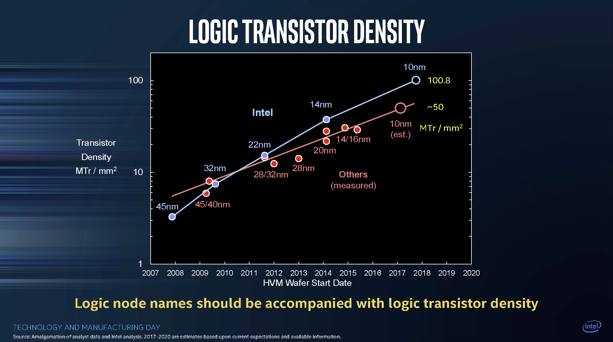
It's this hyperscaling that's making the company unhappy with using process node as a proxy for transistor density. Simply put, Intel's 14nm process offers denser transistors and smaller cells than the 14nm and 16nm processes of its competitors GlobalFoundries, TSMC, and Samsung. Qualcomm is using Samsung's 10nm process for its new Snapdragon 835, and this is set to be the first commercial microprocessor on the market built using a 10nm process. But in terms of actual transistor density, the 10nm Samsung process is comparable to Intel's nearly three-year-old 14nm process. When Intel ships its own 10nm processors later this year, it will again leapfrog the competition.
Accordingly, Intel wants to describe processes in terms of millions of logic transistors per square millimeter, calculated using a 3:2 mix of NAND cells and scan flip flop cells.
Using this metric, the company's 22nm process managed 15.3 megatransistors per millimeter squared (MTr/mm2). The current 14nm process is 37.5MTr/mm2, and at 10nm, the company will hit 100.8MTr/mm2. Competing 14nm/16nm processes only offer around 28MTr/mm2, and Intel estimates that competing 10nm processes will come in at around 50MTr/mm2.
Of course, Intel's competitors, who enjoy the prestige that comes from shipping "10nm" chips ahead of Intel, are unlikely to switch to this metric any time soon.
Listing image by Intel
reader comments
107