Intel Shipping Nervana Neural Network Processor First Silicon Before Year End
by Nate Oh on October 18, 2017 8:00 AM EST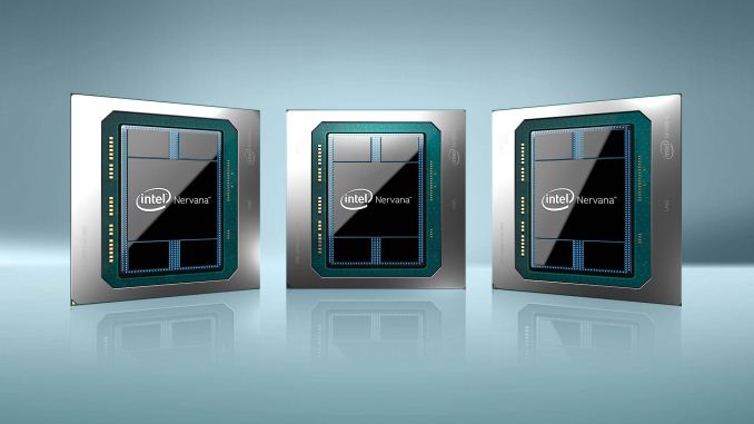
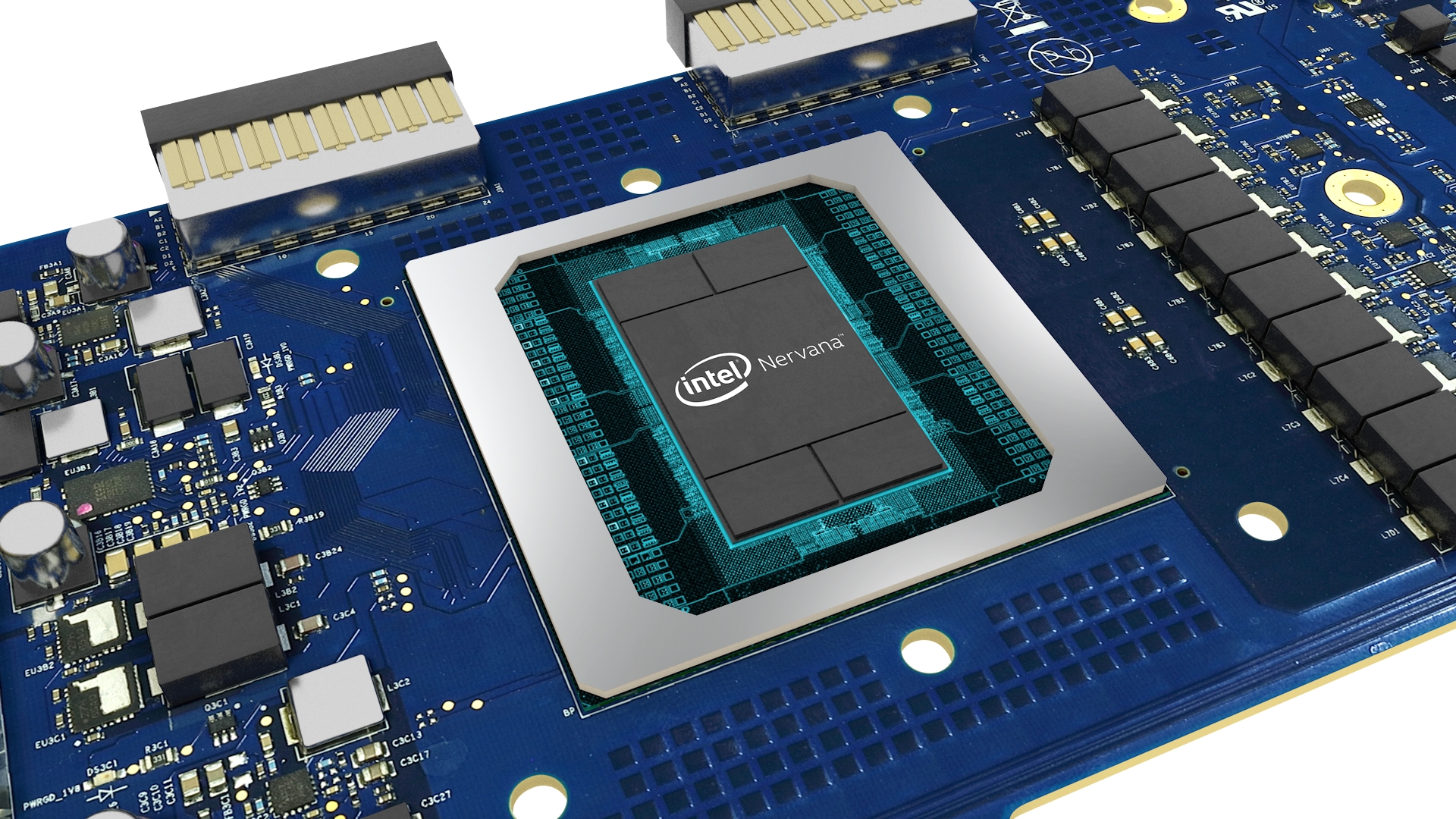
This week at the Wall Street Journal’s D.Live 2017, Intel unveiled their Nervana Neural Network Processor (NNP), formerly known as Lake Crest, and announced plans to ship first silicon before the end of 2017. As a high-performance ASIC custom-designed and optimized for deep learning workloads, the NNP is the first generation of a new Intel product family, oriented for neural network training. From the beginning, the NNP and its Nervana Engine predecessor have aimed at displacing GPUs in the machine learning and AI space, where applications can range from weather prediction and autonomous vehicles to targeted advertising on social media.
Under development for the past three and a half years, the NNP originated as the Nervana Engine deep learning ASIC, which was announced in May 2016 and had all the marquee features of the NNP: HBM2, FlexPoint, cacheless software memory management, and a high-speed interconnect. Not too long after, Nervana was acquired by Intel in August 2016. Later that November during Intel’s AI Day, the Nervana Engine rematerialized to the public as Lake Crest, with first silicon due in 1H 2017. In that sense, the product has been delayed, although Intel noted that preliminary silicon exists today. Nevertheless, Intel commented that the NNP will be initially delivered to select customers, of which Facebook is one. In fact Intel has outright stated that they collaborated with Facebook in developing the NNP.
In terms of the bigger picture, while the past year has seen many announcements on neural network hardware accelerators, it is important to note that these processors and devices operate at different performance levels with different workloads and scenarios, and consequently machine learning performance consists of more than a single operation or metric. Accelerators may be on the sensor module or device itself (also known as on the ‘edge’) or farther away in the datacenters and the ‘cloud.’ Certain hardware may be training deep neural network models, a computationally intensive task, and/or running inference, applying these trained network models and putting them into practice. For Intel's NNP today, the coprocessor is aimed at the datacenter training market, competing with solutions like NVIDIA’s high-performance Volta-based Tesla products.

This segmentation can be seen in Intel’s own AI product stack, which includes Movidius hardware for computer vision and Altera for FPGAs, as well as Mobileye for automotive. The offerings are bisected again with the datacenter, which formally encompasses Xeon, Xeon Phi, Arria FPGAs, and now the NNP. For the NNP family, although the product announced today is a discrete accelerator, the in-development successor Knights Crest will be a bootable Xeon processor with integrated Nervana technology. While Intel referred to an internal NNP product roadmap and mentioned multiple NNP generations in the pipeline, it is not clear whether the next-generation NNP will be based on Knights Crest or an enhanced Lake Crest.
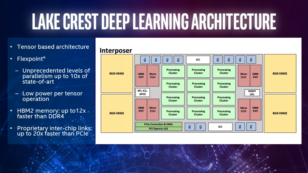
On the technical side of matters, the details remain the same from previous reports. Intel states that the NNP does not have a "standard cache hierarchy," however it does still have on-chip memory for performance reasons (I expect serving as registers and the like). Managing that memory is done by software, taking advantage of deep learning workloads where operations and memory accesses are mostly known before execution. Subsequently, the lack of cache controllers and coherency logic frees up die space. Otherwise for off-die memory, the processor has 32GB of HBM2 (4 8-Hi 1GB stacks) on the shared interposer, resulting in 8 terabits/s of access bandwidth.
Bringing to mind Google's TPU and NVIDIA's Tensor Cores, the NNP's tensor-based architecture is another example of how optimizations for deep learning workloads are reflected in the silicon. The NNP also utilizes Nervana’s numerical format called FlexPoint, described as in-between floating point and fixed point precision. Essentially, a shared exponent is used for blocks of data so that scalar computations can be implemented as fixed-point multiplications and additions. In turn, this allows the multiply-accumulate circuits to be shrunk and the design made denser, increasing the NNP’s parallelism while reducing power. And according to Intel, the cost of lower precision is mitigated by the inherent noise in inferencing.
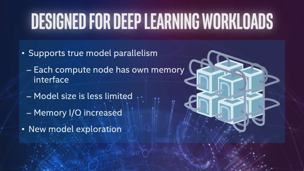
The focus on parallelism continues with the NNP’s proprietary high-bandwidth low-latency chip-to-chip interconnect in the form of 12 bi-directional links. Additionally, the interconnect uses a fabric on the chip that includes the links, such that inter-ASIC and intra-ASIC communications are functionally identical "from a programming perspective." This permits the NNP to support true model parallelism as compute can be effectively distributed, taking advantage of the parallel nature of deep neural networks. Additional processors can combine to act as a single virtual processor with near linear speedup, where, for example, 8 ASICs could be combined in a torus configuration as shown above.
Presumably, the NNP will be fabricated on the TSMC 28nm process that Lake Crest was intended for; just after the acquisition, the Nervana CEO noted that production of the 28nm TSMC processors was still planned for Q1 2017. In any case, 16nm was explicitly mentioned as a future path when the Nervana Engine was first announced, and the CEO had also expressed interest in not only Intel’s 14nm processes, but also its 3D XPoint technology.
Source: Intel


25 Comments
View All Comments
extide - Wednesday, October 18, 2017 - link
If NV gets 100TF on the Tensor cores, and they are claiming 10x .. I wonder if we could see 1PF on this thing!Qwertilot - Wednesday, October 18, 2017 - link
I've a memory that that is 10x Maxwell, so rather less mind boggling :)Yojimbo - Saturday, October 21, 2017 - link
In August of 2016, Naveen Rao, then CEO of Nervana Systems and now, after Intel's purchase of Nervana, VP and GM of the Artificial Intelligence Products Group at Intel, claimed 55 TOPS with the Nervana chip on 28 nm. NVIDIA claims 120 TOPS with the Tesla V100. So in peak theoretical throughput for deep learning operations the V100 seems to have a big advantage.Yojimbo - Saturday, October 21, 2017 - link
Here's the quote, from nextplatform:Think about the performance of the Nervana chip against the Pascal GPU (Nvidia’s top end deep learning and HPC chip, featured in its DGX-1 appliance) in terms of teraops per second, to be exact. A Maxwell TitanX card (which is what they currently use in their cloud for model training) is about six teraops per second, Rao says. Pascal is about double that number, with between 10-11 teraops per second. Nvidia also has a half-precision mode built in as well, which can yield approximately 20 teraops per second, at least based on the numbers he says are gleaned from users that are actively putting Pascal through the paces for deep learning workloads. “On our chip, which is a TSMC 28 nanometer chip, we’re seeing around 55 teraops per second.”
So Qwertilot remembered correctly. They were claiming about 10x Maxwell TitanX.
mode_13h - Wednesday, October 25, 2017 - link
He wants to talk about "teraops per second", but he neglects the smaller Pascals' 8-bit MAC performance? That's like 44 TOPS for GP102.Yojimbo - Wednesday, October 25, 2017 - link
He was talking about training. 8 bit integers don't seem to cut it for training.Drumsticks - Tuesday, October 24, 2017 - link
Volta definitely seems to have a big advantage over Lake Crest. I wonder what they can accomplish moving off of TSMC 28nm though; that's a pretty significant disadvantage by itself. If Intel can wave some money on their fabs and get process parity with Nvidia, that could cut away a big portion of that performance lead. (Maxwell to Pascal was 70% ish without any major architectural changes).Drumsticks - Tuesday, October 24, 2017 - link
And that was with reducing the die size from 398mm (squared) to 314mm. Keeping the die size fixed could probably enable even bigger gains.shabby - Wednesday, October 18, 2017 - link
Does it need a new motherboard?Dr. Swag - Wednesday, October 18, 2017 - link
Why are they manufacturing it at tsmc and not at their own fabs?