
Intel formally announced a new class of Intel Xeon Scalable processors. Codenamed “Cascade Lake-AP” or Cascade Lake Advanced Performance. The disclosure was extremely brief, but it will not stop us from speculating what is happening. Intel Cascade Lake-AP is a new processor with a singular focus: bringing Intel Xeon Scalable back to the forefront of per-socket performance. In this article, we are going to show what Intel disclosed, then speculate on what the company might be doing behind the scenes.
As the AMD EPYC ecosystem has matured, performance and compatibility has gotten better while more systems are now adopting EPYC. Intel is still the market share forerunner so it makes sense that they want a halo product again. AMD is able to claim they have 32 cores and 8 memory channels with the AMD EPYC 7601, while the Intel Xeon Platinum 8180 only has 28 cores and 6 memory channels. Intel wants the halo again, especially since it knows that its 28 core Cascade Lake-SP (successor to the current Skylake-SP) is going to be put under pressure from AMD’s next-generation “Rome” EPYC 2 series.
Background: Intel Cascade Lake-SP
Intel Cascade Lake-SP made its major debut at Hot Chips 30. Here is our article Resetting Scalable Expectations Intel Cascade Lake-SP at Hot Chips 30. In that article we issued a challenge: Intel needed a better story. A new Intel Cascade Lake-AP is that response. In the meantime, here is the basic overview of Cascade Lake-SP.
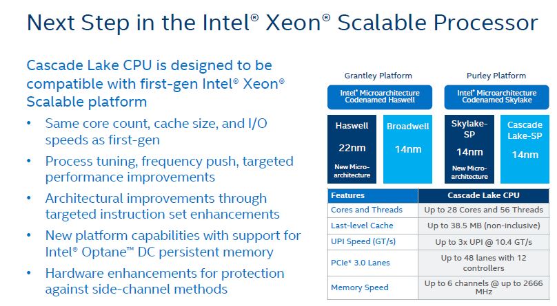
Here we have the same PCIe 3.0 lanes, the same memory speed, the same UPI speed, the same maximum core count and so forth. There are some practical constraints. The LGA3647 socket only has so many pins for PCIe, UPI, and memory channels.
We noted in our previous story that a 28 core Intel Cascade Lake-SP CPU will not be a compelling option as a halo product compared to AMD EPYC “Rome”. Let us take a look at the Advanced Performance disclosure then make some speculation.
The Intel Cascade Lake-AP Disclosure
Intel made a very brief disclosure around Cascade Lake-AP. As a note here, we generally do not put too much weight in the numbers, but we are going to make a leap in our speculation section. Here is the slide Intel showed:
You can see, Intel Cascade Lake-AP is a multi-chip package. We are told that it is a two-chip package so we can infer it is essentially two 24 core chips packaged together. Each package has twice the memory channels of a Cascade Lake-SP part at 12 per package. That yields 24 lanes in a two-socket server which is the same as today’s Skylake-SP four-socket servers.
Although we do not normally comment on benchmark numbers, we wanted to highlight the STREAM Triad “Up to 1.3X” figure. This is absolutely intriguing. AMD EPYC has 8 channels of DDR4-2666 versus Intel Xeon Scalable Skylake-SP or Cascade Lake-SP’s 6 channels. Since the memory speed is the same, AMD claims a two-channel or a 33% advantage over Intel Xeon. The question is: with 12 channels per socket or BGA package, how does one get to a 1.3x memory bandwidth advantage. If we hold DDR4-2666 constant, we have 12 channels for Cascade Lake-AP and 8 channels for AMD EPYC 7601 “Naples.” That would be a 50% advantage or 1.5x the memory bandwidth. Getting to a 1.35x performance factor would imply using 12x DDR4-2400 (Cascade Lake-AP) versus 8x DDR4-2666 (Naples.) This would be truly strange to see memory speeds go down but the math is hard to work out otherwise if one has 50% more memory channels.
Speculation Points Around Intel Cascade Lake-AP
Since the disclosure was so minimal, we are left to speculate what this may be. We specifically did not ask any of our sources about the new parts, this is solely based on the slide above, what Intel has disclosed to STH about Cascade Lake-SP, and some inferencing.
Speculation Point #1: Intel Cascade Lake-AP Cannot Use LGA3647
Since LGA3647 was intended for a single die module with six memory channels and Optane Persistent memory support, it was designed for a time when 48x PCIe lanes and 6 channel memory was a major update over Intel Xeon E5 generations. It was not envisioned to take on something as large as AMD EPYC. There are a limited number of pins, significantly less than AMD uses because Intel does not have as many memory channels nor PCIe lanes to connect. As a result, expanding I/O in the current socket is nearly impossible. To utilize up to 12x memory channels, and if Intel wants to have PCIe leadership or parity again, Intel needs well over 5000 pins.
Further, a 24 core Intel Skylake/ Cascade Lake die uses a lot of power, two would run into a thermal issue even if you accept the notion that the LGA3647 has a much higher TDP than the 205W maximum of the Intel Xeon Platinum 8180 (it does.)
Between needing more pins to connect to memory and PCIe as well as additional thermal headroom needed, we come to our first point of speculation that Cascade Lake-AP will not be based on LGA3647.
Speculation Point #2: New Packaging for 96x or 128x PCIe Lanes
The other intriguing possibility is what happens with PCIe. Intel has the capability to deliver 6x PCIe x16 root complexes per dual die package easily. This is the standard configuration with 48x PCIe lanes per Intel Xeon Skylake-SP generation CPU die. The wildcard is the on-package “PCIe x16” interface used to deliver features such as Omni-Path in the Skylake-SP generation.
You may recall from our 2017 article that Intel has a fourth PCIe x16 solution onboard Skylake-SP, even if it is not widely used. Where the Cascade Lake-AP design could get completely wild is if Intel decides in Cascade Lake to make this more than just an on-package PCIe root and instead exposes it to the outside world.
For LGA3647 servers, this is not a viable path. There are only so many pins available in the package. Cascade Lake-AP, on the other hand, needs to be a larger package to handle the dual die plus already stated 12x DDR4 channels. That gives Intel the opportunity to potentially add pins and add the fourth PCIe x16 complex to the new design. If it does so, it will have 64x PCIe lanes per die, and 128x PCIe lanes per package, or 256x PCIe lanes in a dual Cascade Lake-AP server, bringing it to parity with current generation AMD EPYC. One could argue that such a configuration would go beyond AMD EPYC because the PCH has SATA connectivity and PCIe connectivity which means that the Intel solution would effectively have more lanes than AMD.
If Intel wants PCIe (lane) leadership with Cascade Lake-AP, that is how Intel can get it done with a new socket and a dual package configuration.
Speculation Point #3: UPI Interconnect Is Making This Possible
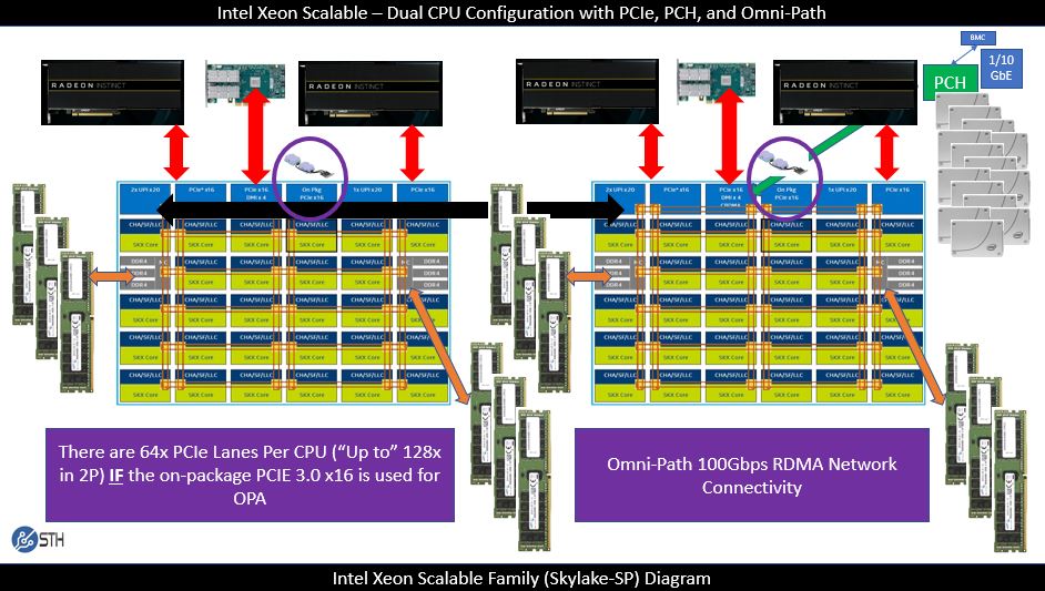
On the call the question was if this solution was using EMIB, a multi-chip packaging technology that Intel is pushing as a path forward. Intel stated that Cascade Lake-AP is not using EMIB and is using UPI. STH readers may recall that UPI is Ultra Path Interconnect and is the technology Intel introduced to replace QPI (Quick Path Interconnect) with Intel Xeon Scalable. Notably, UPI is the technology that is used in dual, quad, and octo socket configurations. Here is the Intel diagram from our Intel Xeon Scalable Processor Family Platform Level Overview.
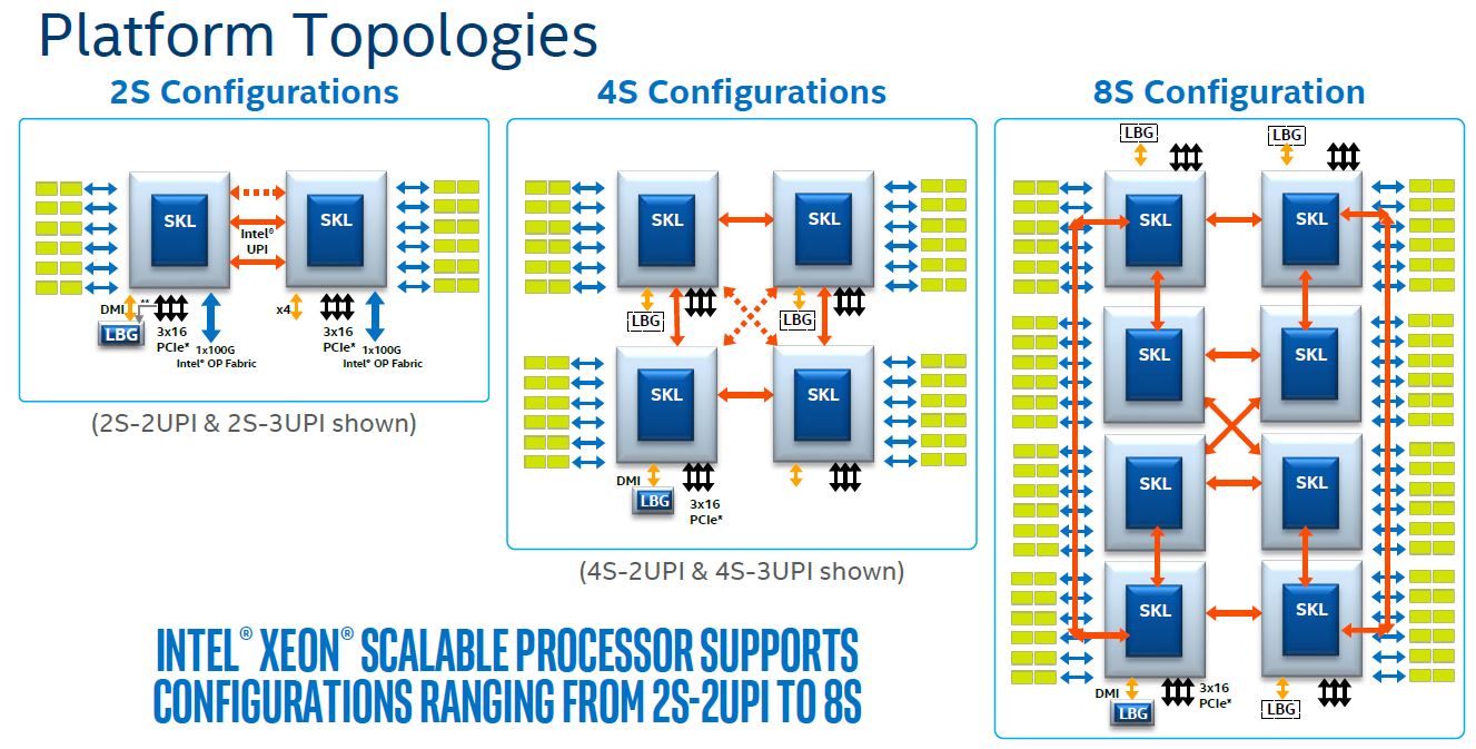
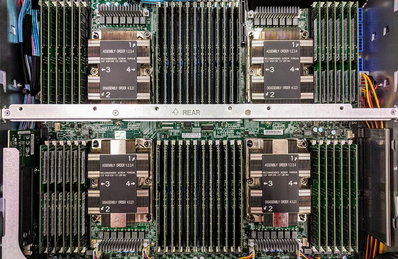
This should look intriguing to our readers. Here is why: take the four-socket configuration, and draw package boxes a bit bigger around two dice instead of just one. Here is an example using a current generation quad socket Intel Xeon Scalable system from Supermicro. Assume that the Cascade Lake-AP dual socket solution will have the capabilities above and below the cross brace bar in a single socket. That is an enormous amount of DIMMs per server.
Assuming one uses 3x UPI CPUs, like the current generation Intel Xeon Gold 6100 and Platinum 8100 generation, one has a potential Cascade Lake-AP product. There are two 24 core chips on a single package with UPI between. There are package-to-package interconnects via UPI as well. Each die has direct access to every other die in a dual CPU configuration. Here is where things get more exciting. Four silicon chips, each with interconnect fabric between them yields a topology like this:
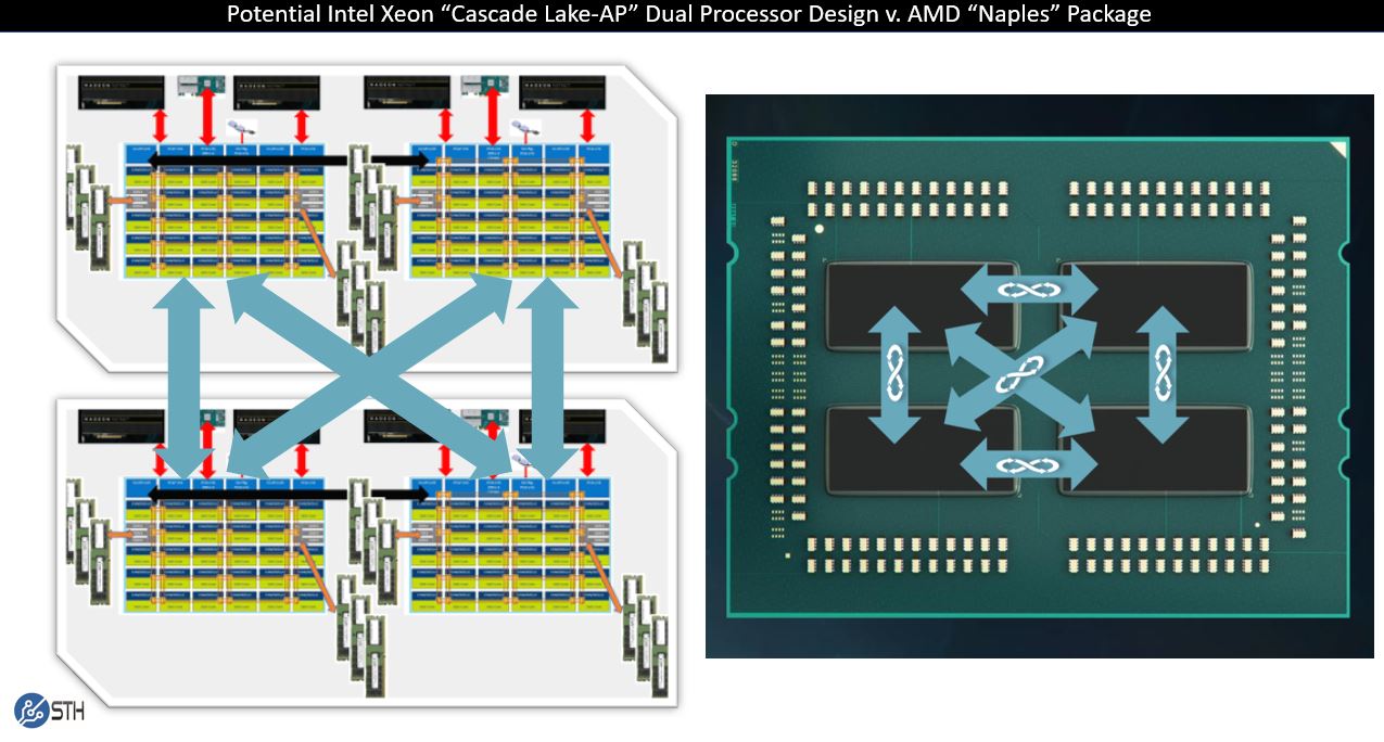
This is the same topology as an Intel Xeon Gold 6100 and Xeon Platinum in the four-socket server shown above, but with two packages instead of four. That is also AMD EPYC “Naples” generation topology, just with UPI instead of Infinity Fabric. UPI is a significantly higher performance interconnect than the first generation Infinity Fabric.
While Intel may have something else going on, and this is all speculation given the extremely limited disclosure, a design like this would allow Intel to use IP blocks and package them differently to claim a much larger per-socket core count, memory channel count, and PCIe count. It would also be a relatively easy design to quickly implement versus building its largest ever CPUs.
Final Words
We have taken Intel’s Cascade Lake building block and barebones Cascade Lake-AP disclosure and gotten to the point where we have a viable halo product once again for the company. We had to speculate on some of the details, which may prove completely incorrect. On the other hand, these speculative points are reasonable if one thinks that Cascade Lake-AP was created quickly as a response to AMD EPYC and did not undergo a long development cycle.
Assuming Intel keeps the full features of the chips, which it can, we can have:
- Dual socket capable design (Intel disclosed this.)
- Two die design with up to 24 cores per die (Intel disclosed this.)
- 12 memory channels per socket (assuming socketed.)
- 96-128 PCIe lanes per processor or 192-256 lanes per system (see Speculation #2)
- A UPI enabled topology similar to today’s four socket Intel Xeon Scalable designs
In the end, this may be a competitive product against today’s’ AMD EPYC 7601. By the time Intel is ready to release Cascade Lake-AP it may find itself competing against a second generation AMD EPYC part with more cores and potentially PCIe 4.0. Intel Cascade Lake-AP is positioned to fight that battle.
If our Speculation #3 is correct, and this is essentially what we would call today’s 4-socket systems re-packaged into a 2-socket design, then this is going to be a relatively easy product to produce. At the same time, it is going to have an enormous impact on software licensing. VMware, as an example, is licensed on a per-socket basis. Using Cascade Lake-AP for VMware will half the cost of VMware licensing versus a quad-socket Intel Xeon Scalable Skylake-SP platform. For those buying per-socket licensed software today, it may be worth assessing what happens to those licenses as Intel and AMD enter into a core war in 2019.


This is a more interesting article than just repeating what Intel said. It makes sense. 2x die on one giant mother of a package and you’d get what they’re describing. Packaging would be a NIGHTMARE and a half tho. So many traces for PCIe, UPI, and memory. You’d need almost a double 3647 and a thicker PCB package or to use a silicon piece like the NVIDIA Tesla V100 GPUs use.
I speculated about Intel doing this as a case of one-upsmanship with AMD. If you instead count the PCIe lanes (48 vs. 16/32) and Memory Channels (6 vs 2) per die Intel is still far ahead of AMD. It will be interesting to see if AMD manages to get more cores per die.
If it’s really just 2 CL die together then they’re stuck at 48 cores. What’s next for AMD? Maybe we’ll see a dual 28 die Intel if EPYC2 has 64 cores. If AMD’s got Gen4 then the PCIe is over for Intel until later in 2019
As was publicly leaked by Intel themselves via a page on their website back in June, Cascade lake AP will use a “socket” called BGA 5903 – wccftech had a working link (I saw it at the time the article went up) but intel took down the page shortly after, at least from public search results.
The TDP of cascade lake AP is expected to top out around 350W, nearly but not quite double that of two current-gen AMD Epyc 7601s (360W) or Xeon 8180s (410W).
Problematically for Intel however, is that Cascade Lake AP is launching around the same time that AMD Epyc gen-2 launches. AMD’s next-gen Epyc will have 64c/128t per socket with a clock bump over current gen Epyc (allegedly capable of reaching into the mid 3ghz range all-cores, but take that one with a grain of salt, since I could not get any solid numbers around this, however the math works out.), with support for potentially greater than DDR4 3200MTS (If AMD can manage 3600MTS support, that gives them bandwidth parity with Cascade lake AP), with a next-gen GMI (on-package) and xGMI (interpackage) interconnect. Its possible that xGMI could bring them up to parity with intel’s UPI. Furthermore, Intel is now saddled with the numa node design that AMD was coping with in 1st gen Epyc, however 2nd gen Epyc does away with that by reinventing the northbridge, just on-package instead of as a discrete component. The ‘northbridge’ die (I’ve seen it called an IO hub, IO complex, IOX die) connects to an arbitrary number of CCX dies. Furthermore, the 7nm 2nd-gen Epyc chips have TDPs well under what cascade-lake AP has, with TDPs expected to top out around 250W. This lends credence to the mid 3ghz all-core clocks, since the 2990WX has a 250W TDP, and is able to reach an all-core clock of 3.4ghz at that TDP under sustained load. With TSMC 7nm providing a power reduction clock for clock greater than 50% vs that of Glofo 14nm/12nm, its possible for a 7nm Epyc package to consume just 250W while hitting around 3.4ghz on all 64 cores.
I’ve seen a leak hinting at a possible 128c/256t engineering sample, which with AMD’s zen2 architecture is entirely feasible to pull off, either with 16 CCX dies connected to an even wider NB/IOX, or with 8 CCX dies still, but now 16 cores per die. However, its also entirely possible that the software was misreading the number of sockets as 1, when it really should have been 2. This engineering sample was clocked at 1.8ghz.
48 isn’t going to be enough.
That licensing point is great from STH. That’ll save us thousands on VMware.
It’ll be interesting to see where Intel prices this, and what motherboards for this end up costing.
Not that we’ll probably see many (any?) boards for these on the open market. Even with “only” 24 DIMM slots, could you even fit a 2P system onto a 12×13 motherboard?
I don’t know that 1P Cascade Lake AP system makes much sense vs a 2P Cascade Lake SP system. They’d have basically the same performance, but the 2P system should be cheaper and more flexible.
Without knowing pricing, it’s hard to know who Intel is trying to sell these to. They make *some* sense for hyperscaling, but I doubt the economics work.
If Rome is 64 cores, a 2P rome might well make a 4P Xeon look bad. This is likely intel trying to get ahead of the narrative, saying “Oh, but we too have something that can consolidate 4P to 2P and lower your TCO, and you *need* 12 channels of memory b/w to feed 48 cores”. Funnily enough, if the rumors are true, Rome will be less NUMA than Cascade Lake AP.
The other way around.
Not one link intra and two inter, but two intra and one inter.
The -AP chips have been previously revealed to be Xeon Phi successors.
While some points are valid, I think they’ll go for 1 DIMM per channel and less flexible I/O for maximum density for those HPC farms.
I tried to calculate UPI bandwidth and am I right that is about 44GB/s ?
If so how much faster it is in reality then Infinity Fabric internal and external links?