In 2019, Intel is going to ship chips using a new 3D stacking technology the company is calling Foveros. Foveros allows complex logic dies to be stacked upon one another, providing a much greater ability to mix and match processor components with optimal manufacturing processes.
Package-on-package stacking is already commonplace in the system-on-chip world. Typically, this involves sticking a memory package on top of a processor, with perhaps a few hundred connections between the two. The size and performance of the connections has limited the application of this technique. With Foveros, the interconnect will use etched silicon (just as EMIB does) to enable many more interconnections, running at much greater speeds.
Foveros follows on from Intel's EMIB (Embedded Multi-die Interconnect Bridge) tech. EMIB is found on the Kaby Lake-G processors that in a single package contain an Intel CPU, AMD GPU, and a chunk of second-generation High Bandwidth Memory (HBM). HBM achieves its high bandwidth by using thousands of interconnects between the GPU and its memory, in comparison to the several hundred used between a GPU and conventional GDDR. The Kaby Lake-G chips use EMIB to provide this connection.
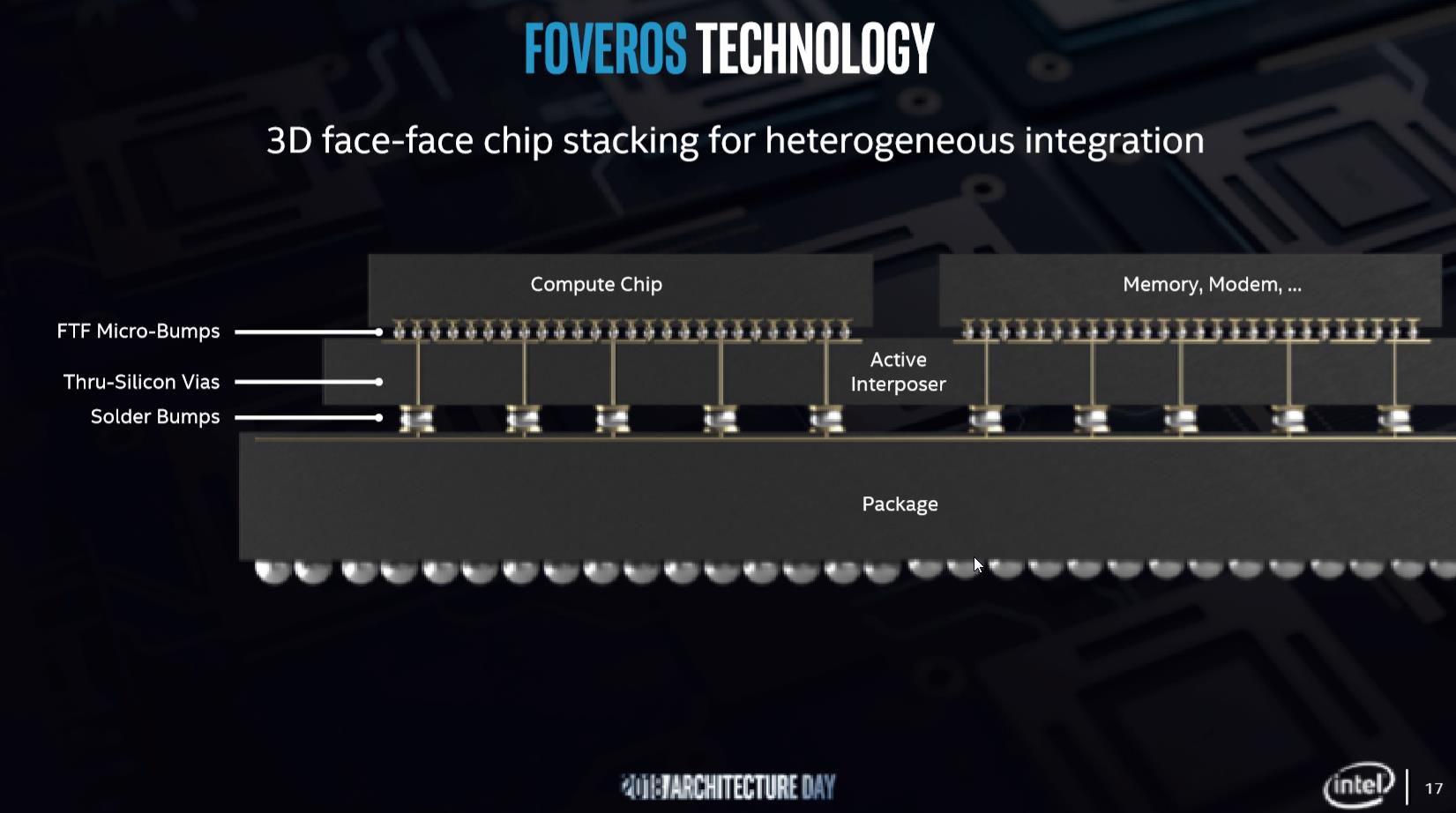
Instead of EMIB's silicon bridges, Foveros uses thousands of "microbumps" on the chip faces, with direct face-to-face connections between the stacked parts. The interposer that the chips connect to isn't just inert silicon with some traces, as in EMIB, but a chip in its own right, with its own logic built in.
The high performance of Foveros means that core processor components can be distributed between different dies. For example, high performance CPU cores might be built on the highest performance 10nm process. But I/O connectivity—integrated USB, Wi-Fi, Ethernet, PCIe—doesn't need all that performance, because it's constrained by the limitations of the physical interfaces it must support. Accordingly, it might make more sense to use a low-power 14nm or even 22nm process for this portion of the chip. Performance will still be good enough, but at much lower power usage or cost than if it had to use the same high-performance process as the logic. Similarly, analog components (for Wi-Fi and cellular connectivity) are optimal on different processes, with different transistor designs. Foveros means that a processor can integrate such components, while still letting them use a process that's optimized for that particular usage.
With EMIB, these different components could be tightly packaged together side by side. Foveros takes that into the third dimension, enabling even greater density and a reduced footprint. Intel anticipates that different CPU tasks will increasingly be split up into chiplets, then combined in a mix-and-match way for the finished chip. Low-power components such as I/O and power delivery will be put into a base die, with high-performance logic stacked on top.
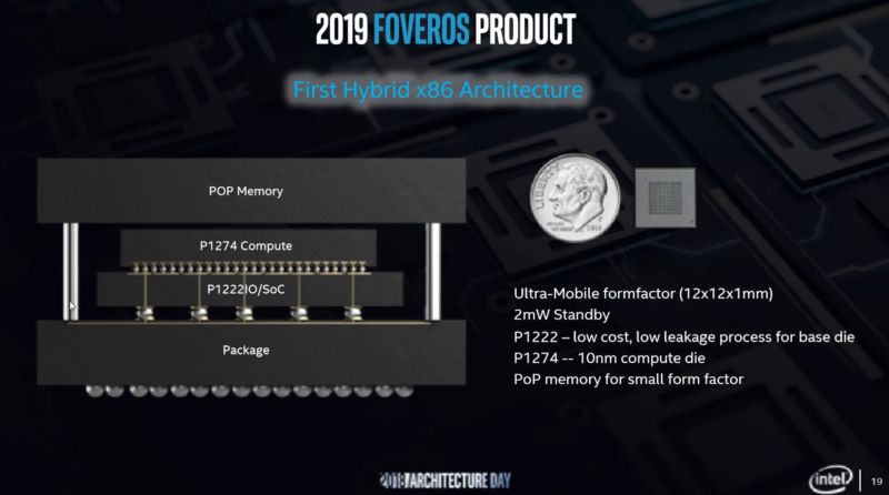
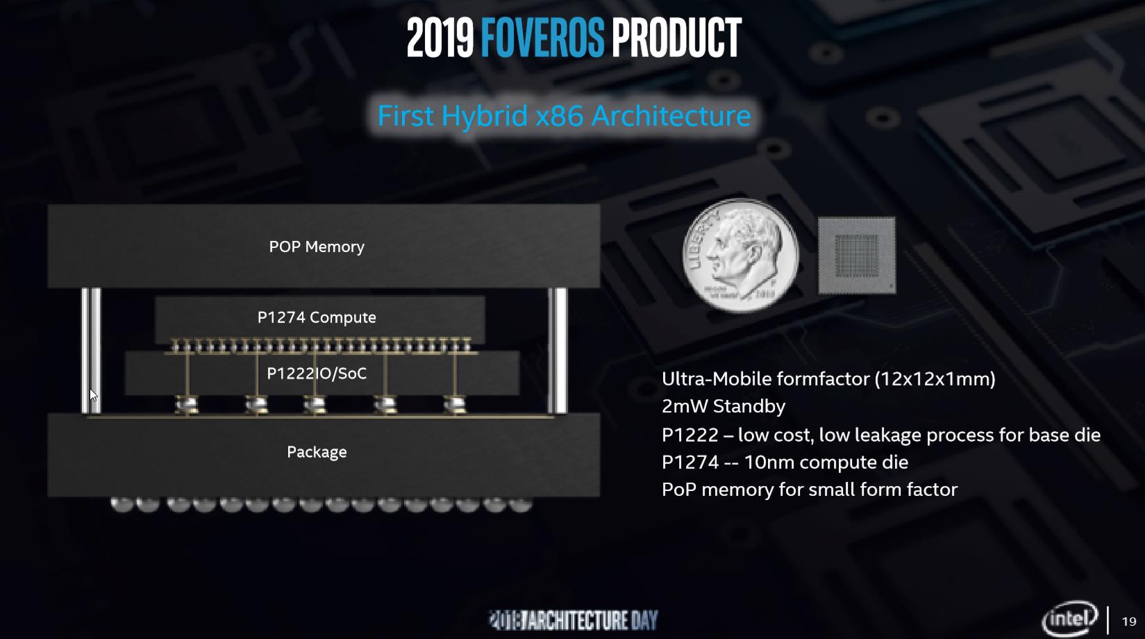
Intel says that Foveros products will be shipping in the second half of 2019 and that the technology is ready for mass-market production—not just specialized or customized processors, but mainstream CPUs. The first products will combine 10nm compute logic stacked on top of a base die using the company's 22FFL (FinFET Low power) process, topped off with package-on-package memory. The 10nm part will contain both a Sunny Cove high power core, and four Atom cores, in a style that is familiar from modern ARM processors: light workloads will be able to use the low power Atom cores, but the Sunny Cove can be powered up for more computationally expensive tasks. This chip will be aimed at ultra-mobile systems with the processor measuring 12×12×1mm and having a standby power of 2mW.
Intel's not the only one to want to use different processes for different bits of a processor. AMD has already announced that its next-generation Zen 2 processors will be separating its CPU logic from I/O. The CPU logic will be on chiplets built on a 7nm process. But everything else—including PCIe, DDR, USB, SATA—will be on a separate 14nm I/O die. AMD will likely be using a conventional multichip module for Zen 2; the different parts will all be connected to a PCB that joins them all together.
reader comments
75