TSMC Pours $19.5B Into Next-Gen 3nm Fabs, Intel Vows To Regain Process Leadership
TSMC 3nm And 5nm Process Nodes
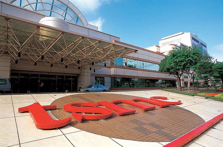
The Electronic Times is reporting that TSMC has just begun construction on its next-generation 3nm fab. The manufacturing line is allegedly being constructed on 74 acres of land within the Southern Taiwan Science and Technology Park. TSMC reportedly has $19.5 billion at stake with its 3nm endeavors, and is expected to begin mass production of chips for customers in 2023.
The 3nm line will be built adjacent to the company’s 5nm line, which entered “risk production” during Q1 2019 and is expected to “tape out” during by Q2 2020. According to TSMC, its 5nm node will be “large and long-lasting”, with most of the company’s current 7nm customers switching over in the coming years. By the time that the 5nm node has run its course, TSMC’s 3nm lines should be up and running.
Intel Looks To “Recapture Process Leadership” In The Coming Years
Given that Intel has been spinning its wheels in the mud with the 14nm process node for what seems like an eternity as it has struggled with the switchover to 10nm, it shouldn’t be surprising to see that TSMC has gained the upper hand. TSMC has already gone through two generations of 10nm SoCs for smartphones (Snapdragon 835, Snapdragon 845) and is currently producing 7nm Snapdragon 855 SoCs.
The company also pumps out 7nm Zen 2-based Ryzen 3000 and EPYC processors for AMD, which has allowed the company to bump up core counts and performance while holding the line on thermals. And TSMC’s 7nm+ EUV process just recently reached volume production (Zen 3, anyone?).

Intel has just dipped its toes in the 10nm waters with Ice Lake-U mobile processors, but the company is looking to get back on track with its tick-tock cadence of process nodes that was thrown completely off kilter in recent years. In the company’s Q3 earnings call last week [transcript], CEO Bob Swan explained that he is confident that Intel will be able to “recapture process leadership going forward.”
“We are accelerating the pace of process node introductions and moving back to a two to two-and-a-half year cadence,” said Swan. “Our process technology and design engineering teams are working closely to ease process design complexity and balance schedule, performance, power and cost.”

He went on to add that in addition to the Ice Lake-U parts that being shipping in Q3, the company has also started shipping 10nm Agilex FPGAs. In the enterprise segment, its 10nm portfolio will expand in 2020 with Xeon CPUs (Ice Lake-SP), an AI Inference Accelerator, 5G Base Station SoC, and its highly anticipated Xe DG1 discrete GPU. Hitting closer to home for our audience, the client side of the 10nm equation will see the launch of Lakefield and Tiger Lakeduring 2020.
“We are on track to launch our first 7-nanometer based products, a data center focused discrete GPU in 2021 two years after the launch of 10-nanometer,” added Swan. “We are also well down the engineering path on 5-nanometer.”