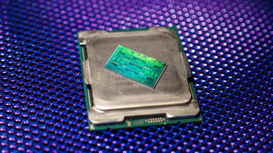
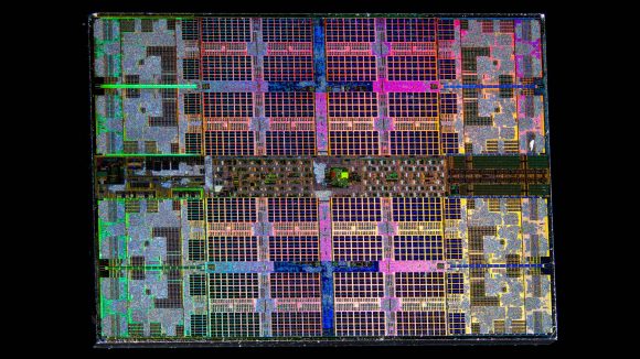
The key to a quick and cheap 7nm product launch for Intel is to take a leaf out of AMD’s book. Over at the Global TMT conference, Murthy Reduchintala, Intel’s chief engineering officer (among numerous other titles), told investors and analysts that roughly 50% of its processor R&D budget is spent on updating non-core logic to the latest process node, and that this has to change in order to ramp up effectively.
That’s by and large the same plan AMD had with Zen 2. While the core clusters, or CCDs, were manufactured by TSMC on its 7nm process, all the non-processing engine silicon – which is responsible for I/O, interconnectivity, and extraneous functions – was shifted off onto a separate 12nm cIOD chiplet manufactured by GlobalFoundries. So in a roundabout way Intel’s pretty keen on replicating this successful, and cheap, heterogeneous approach – which is becoming increasingly more alluring to global chipmakers.
“One of the challenges we always had in the paradigm of monolithic integration is not only do you have to put the IP that benefits from logic scaling, like your processing engines, but you also have to put all of the mixed signal and analogue IP and interconnect IP that requires the connection of those compute ingredients together,” Murthy Renduchintala says.
“And they don’t benefit as proportionately from logic scaling. Therefore, you’re spending about 50% of your R&D on porting technology that doesn’t get the same benefit as logic scaling as your processing engine. Decoupling that and being able to take that with a different cadence makes for a much more higher velocity product roadmap,” he continues.
For an idea of the cash we’re talking here: Intel’s capital investment in 2018 was $15.2bn across the entire business.
With the transition from 14nm to 10nm delayed many times over, the company’s ability to swiftly divert production onto 7nm has been pulled into question. However, Renduchintala expects an adjustment away from monolithic, single-process dies will allow it to meet its ambitious targets.
The split ensures the high-performance process node (which is also sure to be the most expensive) is only used where necessary – and where it’ll prove the most beneficial to performance. Everything else will remain on higher yield technology.
Intel currently relies heavily on 14nm production for most of its business, including all of the best CPUs for gaming from Chipzilla. That’s caused a bit of congestion at the company’s fabs, leading to CPU shortages.
The company is expected to shift more and more production over to the 10nm process node next year, following its initial launch with Ice Lake mobile parts. It’s not until the Ponte Vecchio GPU in 2021 – its first supercomputer-scale GPU – that it will introduce 7nm. Following the launch, all segments will offer some product on the advanced process within a year.
Intel has already touted own-brand technologies, such as Foveros 3D packaging technology and EMIB interconnects, that will allow for hybrid chip designs.
Images courtesy of Fritzchens Fritz, Flickr, CC-0.

