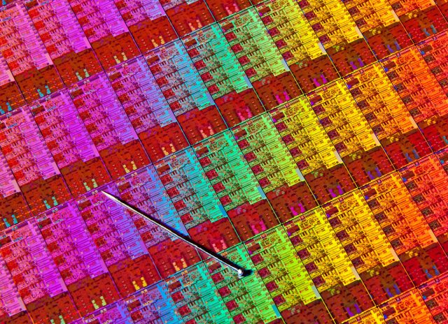
In the semiconductor world, integration is omnipresent, driven by Moore’s Law. Integration reduces power and cost while increasing performance. The latest realization of this trend is the System-on-a-Chip (SoC) approach pervasive among PCs, tablets, and smartphones. And the latest SoC is Haswell.
Haswell is the first new family of SoCs from Intel to target the 22nm FinFET process, which uses a non-planar transistor that wraps around the gate on three sides. While Ivy Bridge was the first family of 22nm products, it was not fully optimized for the 22nm process. The CPU was a shrink of the 32nm Sandy Bridge rather than a new design.
The Haswell family encompasses a new CPU core, a new GPU, and numerous system-level changes. More importantly, it marks the beginning of Intel's more unified approach to SoCs. The Haswell family is really a set of building blocks that architects will assemble for specific markets. The Haswell CPU core is a step forward in performance (as is to be expected from Intel) but more importantly, it is a huge step down in power. This SoC should be viable for high-end tablets. Variants of Haswell are aimed as low as 10W, and future improvements may reduce this further. Intel’s 22nm FinFET node is necessary to achieve this wider range, but it's not sufficient. Haswell's architecture fully exploits the benefits of the new process technology in a way that Ivy Bridge never did. It ultimately yields higher performance and lower power, which will translate into PCs and tablets that run faster with a longer battery life.
At the instruction set level, the Haswell core supports four extensions that profoundly transform the x86 ISA. AVX2 widens integer SIMD (Single Instruction Multiple Data, a form of vectors) to 256-bit vectors, and that adds a gather instruction for irregular memory access. The fused multiply-add (FMA) instructions improve performance for floating point (FP) workloads. For cryptography, networking, and certain search operations, there are new bit manipulation instructions. Lastly, Haswell is the first widely available product with transaction memory through the TSX extension. TSX is an incredibly powerful model for multi-threaded programming that improves performance and efficiency of software by better utilizing the underlying multicore hardware. Microarchitecturally, the Haswell core achieves even higher performance than Sandy Bridge. The improvements are mainly in the out-of-order execution—especially the memory hierarchy. It all strengthens Haswell's case to be the basis of Intel's upcoming generation of products in everything from tablets to servers.
Haswell instruction set and front-end
Haswell introduces four families of new instructions. The first is AVX2, which is a 256-bit extension of existing integer SIMD. It's essentially the counterpart of the floating-point AVX instructions. AVX2 also adds vector permutes and shifts, then gathers, instructions for loading data from non-contiguous addresses. Gather is crucial for compilers to take advantage of wider SIMD instructions (e.g., AVX2 can have 32 byte long elements).
On the floating point side, Intel's new Fused Multiply Add (FMA) extension includes both 256-bit and 128-bit instructions. Compared to the conventional separate multiply and add instructions in SSE, FMA doubles the theoretical throughput. In addition, the fused instructions eliminate the intermediate rounding stage which can improve accuracy for some approximation algorithms.
The third extension is smaller and more focused on integer bit manipulation (known as BMI) for use in cryptography and packet handling. As an aside, Haswell adds a big-endian move instruction (MOVBE) that can convert to and from traditional x86 little-endian format (big-endian data stores the most significant byte first, while little endian stores the least significant byte first). This was originally introduced in Atom, and it was added to ensure full compatibility and improve performance for embedded applications.
The most significant ISA extension is TSX, which has been extensively discussed in a previous article on Haswell's transactional memory. In short, TSX separates performance from correctness for multi-threaded programs. Programmers can write simple code that is easier to debug, while the hardware extracts concurrency and performance.
Coarse-grained locking (e.g., locking an entire data structure) is easy to develop, especially when starting with single threaded code. However, fine-grained locking (e.g., locking a portion of the data structure such as a single node in a B-tree) is almost always higher performance. Hardware Lock Elision (HLE) uses hint prefixes to transparently provide the performance and throughput of fine-grained locking, even when programmers use coarse-grained locks.
Restricted Transactional Memory (RTM) is a new programming model that exposes explicit transactions through new instructions. These transactions can span complex data structures and be composed easily. However, it does require linking new libraries using RTM and possibly rewriting software to get the full benefits.
The new instruction set extensions are clearly the biggest change in Haswell's front-end. At a high level, instruction fetch and decode microarchitecture is largely similar to Sandy Bridge, but there are numerous subtle enhancements to note.
The branch prediction for Haswell has improved, although Intel was unwilling to share the specific details. The instruction cache is still 8-way associative, 32KB, and dynamically shared by the two threads. Likewise, the instruction TLBs are the same capacity. The major changes are enhancing instruction cache misses and prefetching to make better use of the existing resources. Instruction fetching from the instruction cache continues to be 16B per cycle, but with more outstanding L1 misses and more timely prefetching.
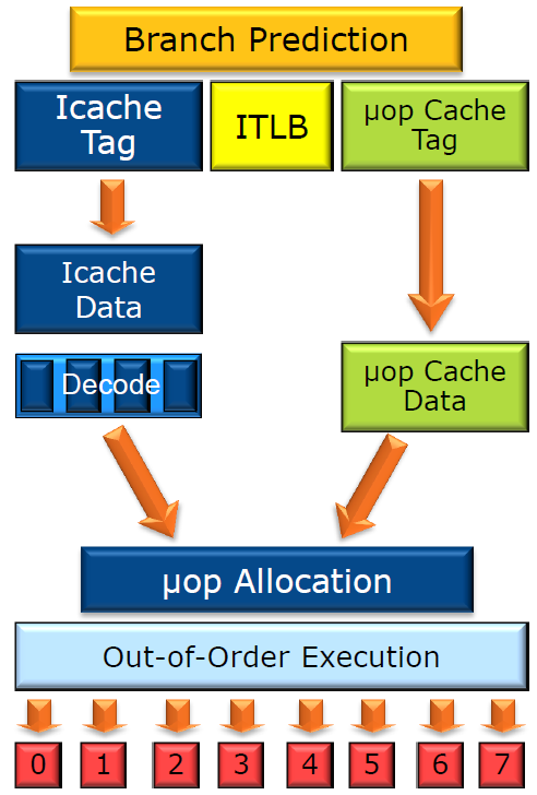
The decoding for Haswell is largely identical to Sandy Bridge. There are four legacy decoders that take in x86 instructions and emit simpler uops. The first is a complex one that can emit 1-4 fused uops and three simple decoders that can emit one fused uop each. Like Sandy Bridge, there is compare+jump fusion and stack pointer elimination. The Haswell uop cache is also identical, with 32 sets of eight cache lines. Each cache line holds up to six uops.
The Haswell uop queue was redesigned to improve single threaded performance. Sandy Bridge had two 28 entry uop queues, one for each thread. However, in Ivy Bridge the uop queues were combined into a single 56 entry structure. The chief advantage is that when a single thread is executing on Ivy Bridge or Haswell, the entire 56 entry uop buffer is available for loop caching and queuing.
reader comments
172