What impresses Asenov about what Intel has done with its 14nm process is its fabrication of a rectangular fin.
“The fabrication is extremely good,” says Asenov, “I was initially disappointed by the Intel 22nm process but, seeing what they’ve done at 14nm, they’ve done a very good job on the fin.”
Two years ago Asenov was the first to point out that the trapezoidal shape of the Intel 22nm finfets is suboptimal and results in stronger short channel effects and in up to 15% reduction in current compared to an ‘ideal’ rectangular finfet.
“First, rectangular gives you better electrostatic control and better short channel effects – it gives stronger sensitivity to channel effect variations,” explains Asenov. “The second thing is how much current can flow through the transistor. The current flow through the top of the transistor is not as high, in a trapezoidal fin, as you would want.”
“It would appear that Intel is a fast learner,” says Asenov. Intel has seen the force of Asenov’s argument and gone for a rectangular fin at 14nm. “I think we may be able to claim some credit for that,” says Asenov.
As a result of the rectangular shape the drive current can, theoretically, be increased.
“It’s very difficult to increase the height of the fin and keep the rectangular shape,” says Asenov. “Simultaneously they’ve increased the height of the fin and the reduction of the pitch gives a 1.7x improvement in the drive current.”
“But,” adds Asenov, “ in these small devices the drive current depends on the contact resistance . So the potential benefit is 1.7x but, if the contact resistance remains the same, the benefit will be small – it may drop to 1.2x or further.”
“The range of expectation could be very good – 1.5x to 1.7x,” adds Asenov, “or it could go back to the same performance as in the previous technology.”
The trouble is we don’t know.
“Intel hasn’t published too much data on the performance of these devices,” says Asenov.
There is another problem with the 14nm process – the SRAM doesn’t scale.
“With Intel’s finfet process, SRAM is very difficult to scale,” observes Asenov. “One of the most unattractive aspects of Intel’s 14nm is that they don’t have proper scaling of SRAM. With finfets the scaling of SRAM is difficult but ST is introducing 14nm SOI almost at the same time as 14nm finfet – and when FD-SOI is introduced at 14nm you can get back to the scaling of SRAM which reduces the cost of the chip.”
“14nm FD-SOI will be 40% cheaper than 14nm finfet,” reckons Asenov.
Asenov is clearly relishing the battle as different technologies fight for supremacy. “I’m glad we’re living in such a very dynamic time – it gives so many opportunities,” he says.
Two such opportunities which have come the way of GSS recently are last November’s licensing of its statistical analysis tools to TSMC and last July’s licensing of tools to Globalfoundries.
On the GSS web-site a post looks at the situation in more detail.
First it cites a report on the achievement of the rectangular fin:

Evolution of the Intel FinFETs from 22nm to 14 nm technology
From a first glance the reduced fin pitch and increased fin height suggest more than 1.7x improvement of the drive current. However the drive current will be strongly affected by the contact resistance and the extrinsic access resistance, both of which are expected to increase with the scaling of the pitch.
GSS has recently simulated very similar rectangular shape FinFETs and the results are published in [1]. The table below compares the geometry of the 14nm Intel FinFETs with the devices simulated in the above paper.
| Intel 14nm FinFETs | FinFETs in [1] | |
| Fin Pich |
42nm |
40 nm |
| Fin Height |
42nm |
44 nm |
| Gate pitch |
70nm |
64nm |
Based on the GSS predictive Ensemble Monte Carlo simulations in [1] illustrated below the ‘intrinsic’ pFinFET drive current of the transistors simulated in the paper can be more than 1.6 mA/mm; Vdd=0.75V. This is based on the assumption that 1.5 GP compressive strain can be introduced in the channel of the simulated transistors by suitable source/drain engineering. The velocity overshoot associated with the non-equilibrium velocity in the channel and the related high degree of ballisticity plays significant role in achieving such performance.
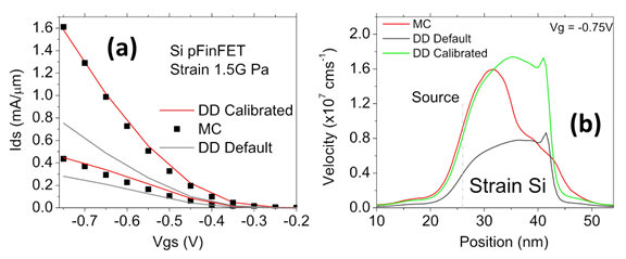
Strained Si pFinFET performance obtained form EMC, (b) Strain Si pFinFET carrier velocity. In the two graphs results of the EMC simulations are compared with results of ‘standard’ TCAD drift diffusion simulations before and after calibration.
However, the Ensemble Monte Carlo simulations do not include the contact and additional access resistances. If an access resistance of 1K ohm is included in the calibrated drift diffusion simulations the drive current drops from 1.6 mA/?m to 1.2 mA/mm. Access resistance of 2K ohm can reduce the drive current to 1.0 mA/mm.
More details about the role of quantum effects, non-equilibrium transport, variability and reliability of the above FinFETs can be found in [1], which can be downloaded from the GSS web page at:
http://www.goldstandardsimulations.com/news/publications/


The idea of a third party reverse engineering company claiming any amount of credit for a process improvement in Intel – based on data from old Intel product – is ridiculous. Such arrogance…