-
Intel has dedicated an ever-larger portion of its chips to the GPU in the last half-decade or so.Intel
-
Intel
-
Intel
-
Intel
This morning's Intel Developer Forum keynote was a bust for anyone hoping for more news about the company's forthcoming Skylake processors. Its chips may make the company most of its money, but CEO Brian Krzanich and crew seem more interested in keynotes-as-forward-looking-spectacles. Interacting with smart vending machines and spider robots get you and your company on late-night TV, but Jimmy Fallon usually doesn't have people on to talk about processor microarchitecture. We get it.
The post-keynote sessions were somewhat more productive. They gave us at least a few architectural details on the Skylake CPUs and their accompanying GPUs, though Intel somewhat frustratingly isn’t using its own developer conference to make specific product announcements. For now, the only GPU we truly know about for sure is the HD 530 that shipped with the high-end overclockable Core i5 and i7 chips (though leaked slides point to a few lower-end mobile GPUs).
Here’s the Skylake graphics breakdown, to the best of our knowledge as of this date. Look for more about the CPUs soon.
The GPUs: However you slice it…
-
Intel
-
Intel
-
Intel
-
Intel
-
Intel
-
Intel
-
Intel
Intel didn’t announce any additional GPUs today, and we don’t know which CPUs are going to be sold with which GPUs just yet. That said, we do have a broad outline of what to expect.
First, a bit about Intel’s GPU architecture in general. They’re intended to be modular and scalable, and Intel can add and remove components to change performance without changing the core capabilities of the GPU.
The GPUs are built from “slices,” each of which usually contains a total of three “subslices.” The subslices usually contain eight “execution units” (EUs) that do the bulk of the processing, texture samplers responsible for grabbing data from memory and passing it on to the EUs, and a few other components. The GPUs also include an “unslice,” a piece outside of the slices that handles fixed geometry and some media functions.
All of this high-level stuff is the same in Skylake as it was in Broadwell, but Intel has made a few specific tweaks. For one, the unslice now has a separate power and clock domain completely independent of the other slices. This means if, say, you’re just using the hardware encoding and decoding capabilities of the unslice, you can completely shut all of the slices down and save power. Additionally, the unslice can run at a higher or lower rate than the slices, improving performance or power usage depending on the specific task you’re doing.
Second, in Broadwell, the company’s GPUs could either use one or two slices, which usually yielded GPUs with either 24 or 48 EUs assuming a slice made up of three subslices with eight EUs apiece (for lower-end or lower-power parts like Celerons, Pentiums, and Atoms, slices can contain fewer subslices and subslices can contain fewer EUs). 24 EU GPUs were referred to as “GT2,” 48 EU GPUs were “GT3,” and 48 EU Iris Pro GPUs with dedicated eDRAM were called “GT3e.”
| Skylake's integrated GPUs | |||
|---|---|---|---|
| Broadwell GPUs | EUs and peak clocks | Replacement Skylake GPUs | EUs and peak clocks |
| Intel HD 5600 (GT2) | 24 @ 1050MHz | Intel HD 530 (GT2) | 24 @ 1150MHz |
| Intel HD 5500 (GT2) | 24 @ 850 to 950MHz | Intel HD 520? | Unknown |
| Intel HD Graphics (GT1) | 12 @ 800MHz | Intel HD 510? | Unknown |
Skylake adds a new three-slice GPU configuration at the top with a total of 72 EUs, called “GT4.” Presumably these will be available with and without eDRAM in GT4 and GT4e configurations. The old GT3e parts, in the form of Iris Pro 5200 and 6200, have already begun working their way up into computers that previously used mid-range dedicated GPUs—things like the base model iMacs and 15-inch Retina MacBook Pro are prime examples. Hypothetical GT4e parts should perpetuate this trend.
What we don’t know is how well this new GPU will scale; we already know that jumping from 24 EUs to 48 EUs doesn’t double GPU performance all by itself. According to our Broadwell benchmarks, the 48 EU HD 6000 is usually around 10 to 20 percent faster than the 24 EU HD 5500 when they’re both using 1600MHz DDR3. Adding eDRAM to alleviate the memory bandwidth bottlenecks can double or triple those scores even without adding more EUs, though, so more EUs paired with eDRAM could produce some impressive results.
Finally, Skylake’s GPUs support either 64MB or 128MB of eDRAM to go with those higher-end GPUs, where Haswell and Broadwell each included 128MB. As in those older architectures, that eDRAM can also be used as a large L4 cache, something which can boost performance for certain tasks even better than added clock speed can. It continues to be a separate die on the CPU package, manufactured on the last-generation 22nm process used for Ivy Bridge and Haswell.
We don’t know how halving that cache is going to affect performance, except to say that adding any amount of eDRAM will be a big improvement compared to the GPUs without it. We can make some educated guesses, though.
In Haswell and Broadwell, there’s a yawning performance gap in between the GPUs with eDRAM and the GPUs without it. Whenever such a gap exists, Intel tends to fire a shotgun blast of products at it, so we could easily see a 64MB GT3e part positioned somewhere in between the no-eDRAM GPUs and a hypothetical 128MB GT4e part. Using less eDRAM could also help Intel get some of these GPUs into smaller systems with less room to dissipate heat.
The good thing about all of this is that there are more options, including (hopefully) eDRAM-equipped GPUs that ship with lower-power CPUs. The bad news is that Intel’s lineup is only going to get more complex and more segmented, which might make it more difficult to find systems that are actually using the combination of CPU and GPU that you want. It’s not a new problem, it just isn’t getting any better with time.
APIs and outputs
-
Intel
-
Intel
-
Intel
-
Intel
-
Intel
Intel’s GPUs have steadily been improving their 4K support over the last couple of years and Skylake’s makes a few more advances in that direction. Like Broadwell, the GPUs will support 4K output at 60Hz over DisplayPort 1.2 or Embedded DisplayPort 1.3, 4K output at 24Hz over HDMI 1.4, and 4K output at 30Hz over Intel’s Wireless Display or the Miracast protocol.
New to Skylake is kind-of-sort-of support for HDMI 2.0, which provides the bandwidth necessary to push 4K screens at 60Hz. It has to be pushed out via a DisplayPort to HDMI 2.0 adapter, though, and we don’t yet know if there are specific requirements that dictate what kind of adapter you need to use. Intel will also support HDMI 2.0 over Thunderbolt 3, for the systems that include the controller.
Intel’s integrated GPUs can still drive up to three displays at once, though the resolutions and refresh rates supported simultaneously are still unknown and will likely differ according to the GPU you have.
Skylake also expands hardware-accelerated encoding and decoding support. It can encode and decode 8-bit H.265/HEVC content, which its predecessors couldn’t do, and it adds hardware encoding support for the JPEG and MJPEG formats. Some of this work is performed by the GPU itself, while some can be handled by the lower-power multi-format codec in the GPU’s unslice. Notably, H.265/HEVC decode is supported by the unslice, which should be good for power usage if you’re just streaming video (encoding requires firing up the GPU).
Finally, there are a few changes at the API level. Skylake supports DirectX 12, OpenGL 4.4, and OpenCL 2.0 as of this writing, and Intel’s slide deck claims it should be able to support future OpenCL 2.x versions, OpenGL 5.x, and the low-overhead Vulkan API in the future.
It’s worth noting that Intel’s latest drivers bring some of these improvements to Broadwell and Haswell, though—Broadwell currently supports DirectX 12, OpenGL 4.3, and OpenCL 2.0, while Haswell supports DirectX 12, OpenGL 4.3, and OpenCL 1.2. Other APIs may be added to these older GPUs in future driver updates, so don’t feel like you need to jump on Skylake solely for the graphics API enhancements.
Memory bandwidth
One of the biggest problems for integrated GPUs is memory bandwidth—they’re using the same RAM as the rest of the system, and by nature it’s not as fast as the stuff that’s used on dedicated graphics cards.
One way this gets boosted in Skylake is straightforward: boost the speed of the system memory. Skylake CPUs support 1866MHz and 2133MHz RAM, depending on the SKU, and as we go forward DDR4 should provide even higher speeds.
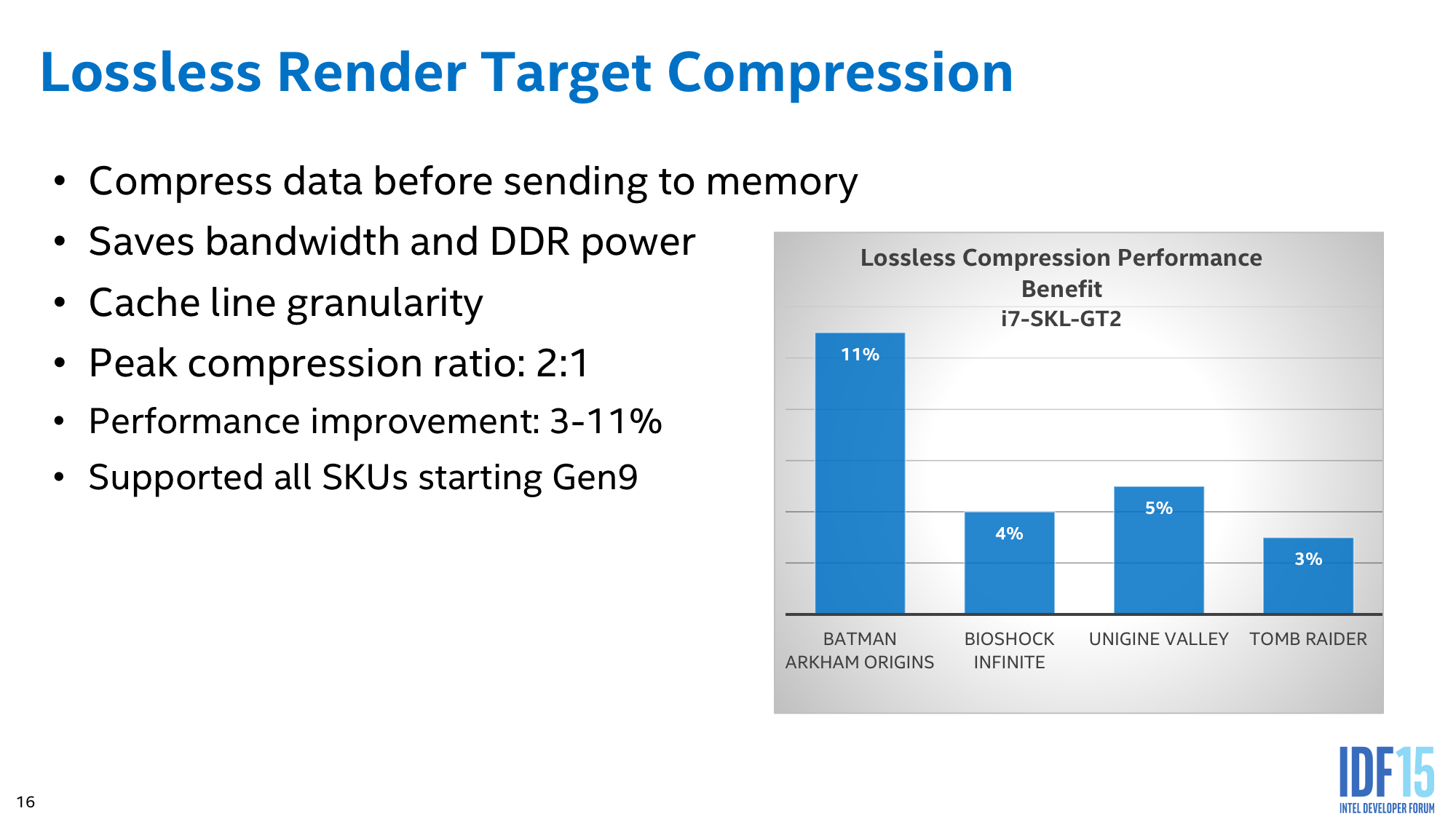
All of the Skylake GPUs also add a feature Intel calls “Lossless Render Target Compression.” The idea is to compress data before sending it to RAM, leaving more bandwidth left for other things. Though at its peak data can be compressed to half its size, the performance improvements are more modest. Intel’s gaming data shows gains between 3 and 11 percent depending on the game, and smaller increases seem to be the more common ones.
Other improvements
-
Intel
-
Intel
Those of you interested in digging deeper into specific changes Intel made for Skylake’s GPUs can go straight to the source—the slide deck from today’s IDF presentation is here (PDF), and a whitepaper with more details (including more on the basic building blocks of Intel’s GPUs and the capabilities carried over from previous architectures) is here (PDF).
Here are a few of the smaller but interesting additions Intel has made:
- Intel has improved the speed of the 2x, 4x, and 8x multisample anti-aliasing modes, and has added support for 16x MSAA.
- Each slice can now access 768KB of L3 cache, up from 512KB in Broadwell.
- There have been significant improvements to "preemption granularity," or the speed with which the GPU can dump a task so it can turn around and do something else. Intel claims the preemption is good enough that touch input can be GPU-accelerated.
- The "ring bus" that allows the GPU, CPU, L3 cache, and system agent to communicate with one another can either communicate more quickly when it's running at the same frequency, or can communicate at the same speed while reducing frequency (and thus power usage).
Now that we know the basic features of the Skylake GPUs, we need to know how the various GPUs differ from one another in clock speed, EU count, and other features. We need to know what CPUs you can pair with what GPUs, and the power requirements for all of them. We'll continue to report as Intel releases more specific product information.
Listing image by Intel
reader comments
65