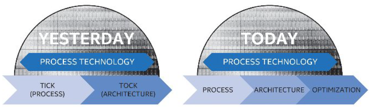
It looks like the Kaby Lake processor isn't a one-off. Intel's latest 10-K filing (spotted at Motley Fool) discloses that the two-phase "tick-tock" development model that the company has been using since 2007 is being replaced with a three-phase model: Process, Architecture, Optimization.
Under tick-tock, development was split into "ticks," where an existing processor design would be migrated to a new manufacturing process, and "tocks," where a new processor design would be released onto an existing process. The process has been used since Intel first introduced its "Core" branded processors, and the model has created a familiar pattern. Each tock introduces new features and improved architectural performance, and each tick has improved power consumption and/or clock speeds.
However, the process has come under increasing pressure. It took Intel a long time to ramp up production on the 14nm manufacturing process used by the Broadwell (tick) and Skylake (tock) processors, with Broadwell in particular suffering from an extremely long and drawn-out roll out and availability. Broadwell was delayed, with its initial late 2013 release pushed back to September 2014. The Broadwell line-up was incomplete—Intel didn't create a full range of desktop processors—and even with the delays, nine months passed between when the first mobile parts were released and the limited selection of desktop processors came out. A couple of months later, Skylake hit the market.
Reacting to these difficulties, Intel announced last July that it was breaking from the tick-tock pattern on 14nm. Skylake was originally going to be replaced with Cannonlake, a tick that would see the manufacturing process shrink from 14nm to 10nm. The new plan is to introduce a third generation of 14nm processors, called Kaby Lake, before shrinking that to 10nm in the second half of 2017.
The 10K says that Intel has a similar plan at 10nm, extending its life from two generations to three. With this three generation process now apparently being the new normal, Intel has given the steps names. The first two stages are familiar, just renamings of the tick-tock plan. The first stage is "process," where an existing design is lightly modified in order to shrink it onto a small process. This is followed by "architecture," where a new architecture is introduced. The new third stage is "optimization," where that architecture is revised. With this new plan, Intel says that it will be able to get back on track with annual product refreshes.
The switch is driven by two related factors: cost and complexity. Each new process is getting harder to develop and productionize. It took Intel much longer to manage acceptably high yields on its 14nm process than it did on the predecessor 22nm process. This difficulty is only going to continue. The features on each processor are now substantially smaller than the light wavelength (193nm ultraviolet (UV)) used to "print" the layout onto the process. A number of techniques are used to accommodate this mismatch, but they add time and complexity to manufacturing.
Since the late 1990s, the industry has been hoping to switch to a smaller wavelength—13.5nm extreme ultraviolet—but production quality systems remain out of reach. Intel's 10K notes that it is continuing to provide research and development funding to Dutch firm ASML, an important developer of extreme UV (EUV) technology, but the implication is that this hardware is still some way off. The funding will be provided over the next five years. Intel is also working on switching from 300mm wafers to 450mm—another change that has been talked about for a long time, but never actually materialized.
This complexity in turn makes it uneconomical to drop a process after a two-year cycle. Extending to a three-year cycle means that Intel can get more out of its investment.
Intel's new development process raises the question of whether the company will be able to maintain its manufacturing advantage over chip fabricators such as TSMC and Global Foundries. Perhaps even more than its processors, it's Intel's manufacturing process that has been world-leading, with the company quick to adopt process shrinks and advanced techniques such as 3D gates and boasting of low power consumption, high transistor density, and high yields even for large chips. IBM has demonstrated a 7nm chip using EUV lithography, and TSMC may introduce 7nm in 2018. As such, Intel may find itself leapfrogged, at least when it comes to one aspect of chip manufacturing.
reader comments
146